Detectors
In the context of spectrophotometers, the term "detector" refers to a light-receiving element that absorbs the energy of light and consequently induces an electrical change. Types of photoelectric conversion include the external photoelectric effect, a prominent form of which is photoelectric emission from a photoelectric surface into a vacuum, and the internal photoelectric effect, in which photoelectrons are excited into a conduction band. One representative example of a detector based on the former type of photoelectric emission is the photomultiplier tube. Here, of the various aspects of spectrophotometers described in UV Talk Letter Vol. 2, "The Structure of a Spectrophotometer," we will look more closely at these "detectors."
1.Introduction
The mechanism for sensing light and converting it to signals that we are most familiar with is the human optic nerve. The human eye senses light in a wavelength range of approximately 400 to 700 nm, and sends signals to the brain through nerve tissue. You could say that the eye is the optical detector of visible light that we are most familiar with. The human eye is sensitive to light in the visible region, and is most sensitive to green light with a wavelength of around 550 nm. In the same way, the detectors in spectrophotometers also have a wavelength range that they can be used for, and their sensitivity varies with the wavelength. Representative detectors with sensitivity in the ultraviolet and visible region include the photomultiplier tube and the silicon photodiode. Regarding near-infrared detectors, PbS photoconductive elements were used exclusively in the past, although nowadays there are instruments in which InGaAs photodiodes are used for part of the near-infrared region. Fig. 2 shows the relationship between various detectors and wavelength ranges.
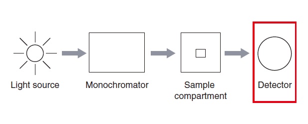
Fig.1 Structure of a Spectrophotometer
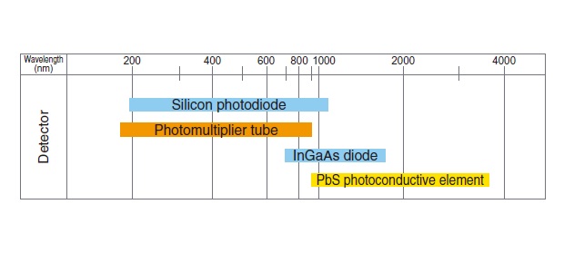
Fig.2 Detectors and Wavelength Ranges
2. Photomultiplier Tube
A photomultiplier tube utilizes the external photoelectric effect, the phenomenon whereby photoelectrons are discharged when light strikes a photoelectric surface. Fig. 3 illustrates the operating principle of a photomultiplier tube. Photoelectrons discharged from a photoelectric surface (i.e., primary electrons) cause the successive emission of secondary electrons from dynodes (electron-multiplier electrodes) arranged in multiple stages, and this cascade ultimately reaches an anode. If one primary electron causes the emission of δ secondary electrons, and this process is repeated n times, then a multiplication factor of δn is obtained. Because photomultiplier tubes ultimately produce a large output for a low level of light intensity, their most important feature is that they offer an outstanding level of sensitivity, which cannot be obtained with other optical sensors. δ is referred to as the "secondary emission coefficient." A high voltage (-HV) is applied from outside the tube in order to accelerate the electrons.
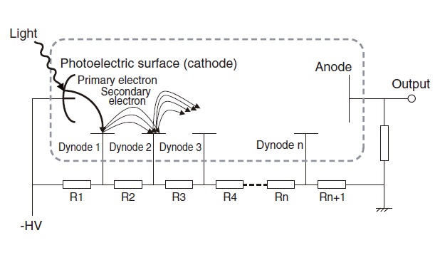
Fig.3 Operating Principle of Photomultiplier Tube
The higher the value of this voltage, the larger the secondary emission coefficient. Another feature of a photomultiplier tube, then, is that the multiplication factor can be adjusted by controlling this high voltage. If there is sufficient light intensity, the voltage is decreased. If the light intensity decreases, the voltage is increased. If the slit is changed, or if accessories that cause significant decreases in light intensity, such as integrating spheres, are used, the advantages offered by this photomultiplier tube become particularly important. For this reason, photomultiplier tubes are used in high-grade instruments.
The relationship between the sensitivity of a photoelectric surface and the wavelength of incident light is referred to as the "spectral sensitivity characteristic." It is mainly determined by the material of the photoelectric surface. Fig. 4 shows the spectral sensitivity characteristic of a multi-alkali photoelectric surface that has sensitivity in the ultraviolet and visible region.
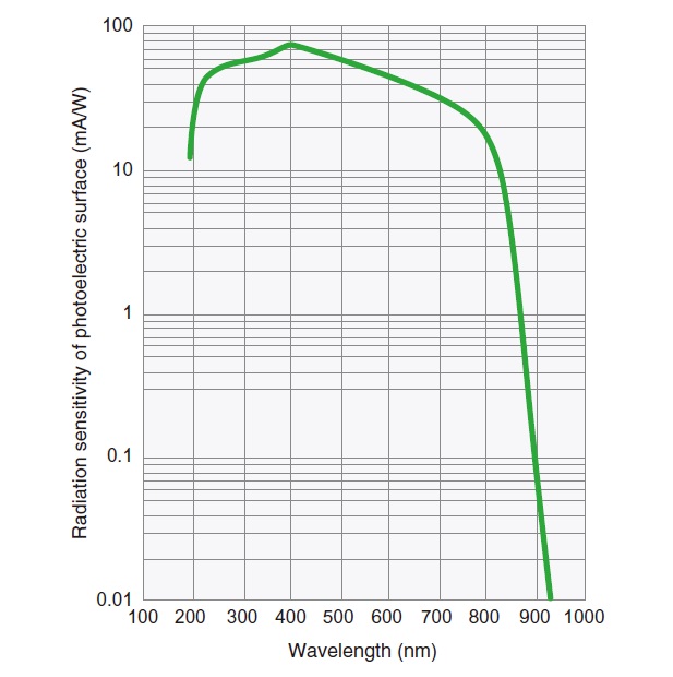
Fig.4 Spectral Sensitivity Characteristic of Photomultiplier Tube2)
3.Silicon Photodiode
A silicon photodiode utilizes the internal photoelectric effect, the phenomenon whereby the electrical properties of the detector itself change when light strikes it. As the name suggests, a silicon photodiode is a semiconductor. When light strikes this semiconductor, if the energy of the light is larger than the band gap, electrons in the valence band are excited into the conduction band, and holes are left in the original valence band. As shown in Fig. 5, these electron-hole pairs are created throughout the semiconductor, but in the depletion region, the electric field causes electrons to be accelerated toward the Nregion and holes to be accelerated toward the P-region. As a result, electrons accumulate in the N-region and holes accumulate in the P-region, and the two regions become, respectively, negatively and positively charged. If this is connected to a circuit, current flows.
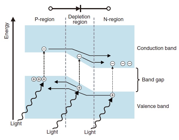
Fig.5 Energy Model of Silicon Photodiode
The band gap of silicon is approximately 1.12 eV, so current flows only for wavelengths that have an optical energy greater than this. This works out to a wavelength upper limit of around 1,100 nm. Fig. 6 shows the spectral sensitivity characteristic of a silicon photodiode.
Silicon photodiodes have some advantages over photomultiplier tubes: they are less expensive; there is little unevenness of sensitivity over their light-receiving surfaces; and they do not require a dedicated power supply. Even with respect to sensitivity, if the light intensity is relatively high, they can provide photometric data that is by no means inferior to that obtained with photomultipliers. If the light intensity is relatively low, however, because signals are amplified in the electronic circuit that gives a current, increasing the amplification factor decreases the response speed.
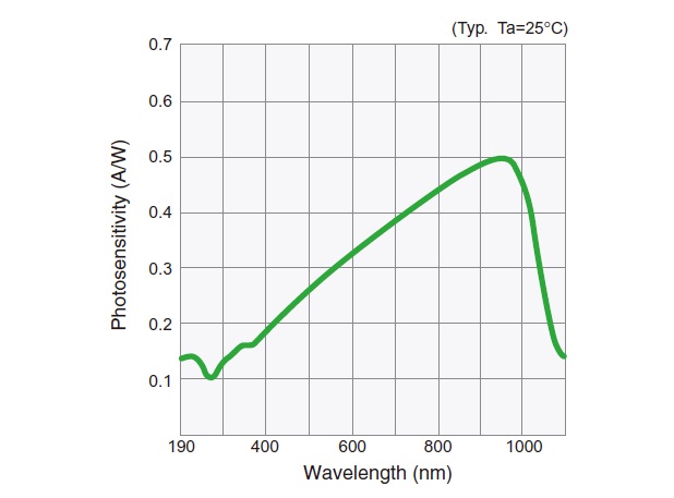
Fig.6 Spectral Sensitivity Characteristic of Silicon Photodiode3)
4. InGaAs Photodiode
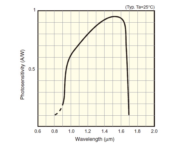
Fig.7 Spectral Sensitivity Characteristic of InGaAs Photodiode3)
Indium gallium arsenide (InGaAs) is a compound semiconductor. Like a silicon photodiode, an InGaAs photodiode is a photovoltaic element that has a P-N junction. The band gap energy of InGaAs, however, is smaller than that of silicon, so it absorbs light of longer wavelengths. This means that InGaAs photodiodes are sensitive to wavelengths that exceed the range of silicon photodiodes. Fig. 7 shows the spectral sensitivity characteristic of an InGaAs photodiode.
5. PbS Photoconductive Element
A photoconductive element is a photoelectric conversion element that utilizes the phenomenon of photoconduction, whereby the electrical conductivity (resistance) of a material changes when it is irradiated with light. Fig. 8 illustrates the operating principle. When light of energy greater than the energy gap between the conduction band and the valence band strikes the element, electrons in the valence band are excited into the conduction band, and holes are created in the valence band. With a PbS photoconductive element, the resistance is reduced in accordance with the intensity of incident light, and this is obtained as a signal using an external circuit.
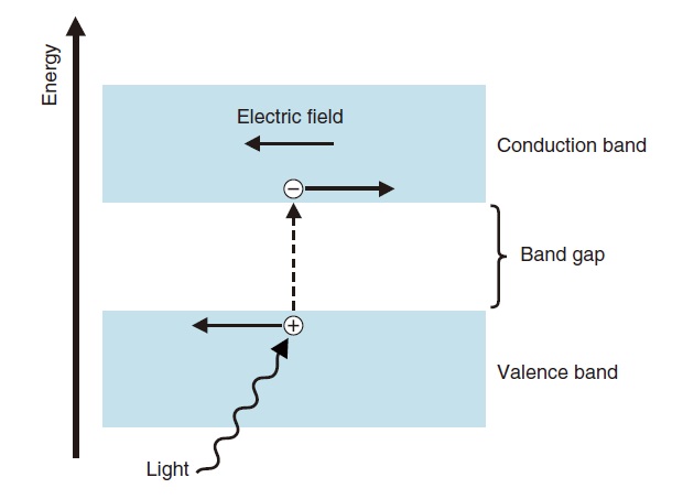
Fig.8 Operating Principle of Photoconductive Element
If the element is cooled, the spectral sensitivity characteristic shifts to the long-wavelength end; as a result, the element becomes more sensitive to longer wavelengths. At the same time, however, the response speed decreases. Although PbS photoconductive elements can, unlike some other nearinfrared detection elements, be used at room temperature, they are still delicate elements for which the sensitivity, response speed, and dark resistance change according to the temperature. Fig. 9 shows the spectral sensitivity characteristic of a PbS photoconductive element.
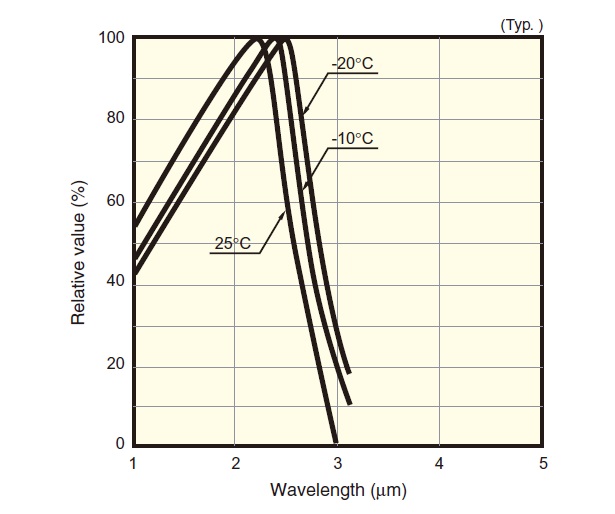
Fig.9 Spectral Sensitivity Characteristic of PbS Photoconductive Element3)
6. Summary
Here, we have looked at detectors that convert light to electrical signals.
Although it does not require consideration in the analysis of solution samples, when performing transmission measurement for solid samples of a certain thickness, such as glass plates and lenses, the form of the light beam that strikes the detector may vary according to whether or not the sample is present. In this case, unevenness of sensitivity over the detecting surface of the detector can cause measurement errors. An accessory called an "integrating sphere" allows measurement to be performed without being influenced by this unevenness of detector sensitivity.
In the next issue, we plan to provide a more detailed explanation of this integrating sphere, which can be described as part of the detector. I look forward to your continued interest.
- 1) Lecture text from Shimadzu course on absorption spectrometry:
"Operating Principles, Structure, and Applications of Spectrophotometer" (Shimadzu Corporation) - 2) Hamamatsu Photonics Photomultiplier Brochure
- 3) Hamamatsu Photonics Opto-Semiconductor Element Brochure